Chapter 1. Research Objective
1.1 Objective, Definition & Scope
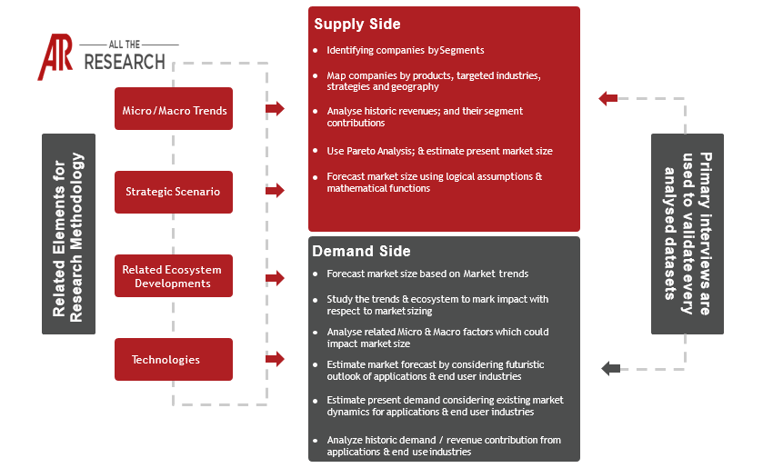
1.2 Methodology
1.2.1 Primary Research
1.2.2 Secondary Research
1.2.3 Market Forecast - Estimation & Approach
1.2.4 Assumptions & Assessments
1.3 Insights and Growth - Relevancy Mapping
1.3.1 FABRIC Platform
1.4 Data mining & efficiency
Chapter 2. Executive Summary
2.1 Semiconductor Metrology / Inspection EquipmentMarket Overview
2.2 Interconnectivity & Related markets
2.3 Ecosystem Map
2.4 Semiconductor Metrology / Inspection EquipmentMarket Business Segmentation
2.5 Semiconductor Metrology / Inspection EquipmentMarket Geographic Segmentation
2.6 Competition Outlook
2.7 Key Statistics
Chapter 3. Strategic Analysis
3.1 Semiconductor Metrology / Inspection EquipmentMarket Revenue Opportunities
3.2 Cost Optimization
3.3 Covid19 aftermath - Analyst view
3.4 Semiconductor Metrology / Inspection EquipmentMarket Digital Transformation
Chapter 4. Market Dynamics
4.1 DROC
4.1.1 Drivers
4.1.2 Restraints
4.1.3 Opportunities
4.1.4 Challenges
4.2 PEST Analysis
4.2.1 Political
4.2.2 Economic
4.2.3 Social
4.2.4 Technological
4.3 Market Impacting Trends
4.3.1 Positive Impact Trends
4.3.2 Adverse Impact Trends
4.4 Porter's 5-force Analysis
4.5 Market News - By Segments
4.5.1 Organic News
4.5.2 Inorganic News
Chapter 5. Market Segmentation
The Semiconductor Metrology / Inspection EquipmentMarket has been analysed to include the below segmentation:
By Types
• Lithography Metrology
• Wafer Inspection
• Thin Film Metrology
• Other Process Control Systems
Chapter 5A. Regional Segmentation
The Semiconductor Metrology / Inspection EquipmentMarket has been analysed by studying the following regions:
North America
• By Types
Europe
• By Types
APAC
• By Types
LatAm
• By Types
MEA
• By Types
**The Regions are further studied to analyse the major countries within the respective regions. The coverage of the country level data is dynamic and is updated regularly based on the market movements. Normally, the countries covered in the report include:
• North America - United States, Canada, Mexico;
• Europe - United Kingdom, France, Italy, Germany, Spain, Rest of Europe;
• Asia Pacific - China, India, Japan, South Korea, Rest of APAC;
• Middle East & Africa - South Africa, GCC Countries, Rest of MEA;
• Latin America - Brazil, Argentina, Rest of LatAm;
Chapter 6. Market Use case studies
Chapter 7. KOL Recommendations
Chapter 8. Investment Landscape
8.1 Semiconductor Metrology / Inspection EquipmentMarket Investment Analysis
8.2 Market M&A
8.3 Market Fund Raise & Other activity
Chapter 9. Semiconductor Metrology / Inspection EquipmentMarket - Competitive Intelligence
9.1 Company Positioning Analysis
9.1.1 Positioning - By Revenue
9.1.2 Positioning - By Business Score
9.1.3 Legacy Positioning
9.2 Competitive Strategy Analysis
9.2.1 Organic Strategies
9.2.2 Inorganic Strategies
Chapter 10. Key Company Profiles
*The Semiconductor Metrology / Inspection EquipmentMarket Report profiles companies based on the material impact they have on the market ecosystem. These are hence, to be read as 'Key Players' and not necessarily 'Market Leaders'.
Companies are typically profiled to include:
10.x.1 Company Fundamentals
10.x.2 Performance Overview
10.x.3 Product Overview
10.x.4 Recent Developments
Key Companies profiled in this report include:
• Kla Corporation
• Applied Materials Inc.
• Onto Innovation Inc. (Rudolph Technologies Inc.)
• Thermo Fisher Scientific Inc.
• Hitachi Hi-Technologies Corporation
• Nova Measuring Instruments
• Asml Holding Nv
• Lasertec Corporation
• Jeol Ltd
• Nikon Metrology Nv
• Camtek Limited
Chapter 11. Appendix
11.1 About AllTheResearch (ATR)
11.2 ATR Services
11.3 Author details
11.4 Terms & Conditions
11.5 Contact us


